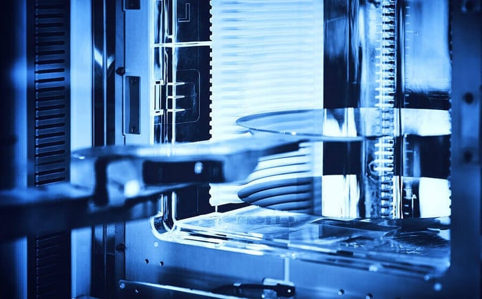
Automated loading and unloading of CMP polishing machines in wafer production

Application and Solution
Maximum precision for flawless wafer surfaces – chemical-mechanical polishing (CMP) is a crucial step in the semiconductor manufacturing process. A uniform and flawless polish is essential to ensure optimal conditions for the subsequent photoresist coating and exposure. To make this delicate process efficient and automated, we work with our automation partners to offer fully automatic systems for loading and unloading wafers into and out of polishing machines.
With our camera-based solution, we automatically detect different types of carrier rings on the polishing cloth, control and check the correct positioning of the wafers to be polished in the carrier ring via robot, and also control a fully automatic removal of the wafers via robot.
Characteristic
- Automatic identification of different types of carrier rings
- Automated loading of wafers into the polishing machine by determining the nest positions in the carrier ring with an accuracy of 50µm
- Checking that all wafers are correctly placed in the carrier ring (no overhang or overlap)
- Automatic position detection of the polished wafers after the polishing process for automatic removal by robot
Advantages

